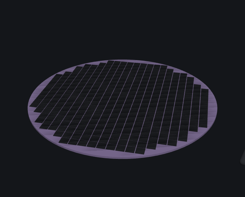
The wafer
Before it becomes hundreds of chips, silicon is a disc polished like a mirror.
Before it becomes hundreds of chips, silicon is a disc polished until it mirrors your face. The standard wafer is 300 mm across and 775 µm thick: wider than a plate, thinner than a credit card. It is cut from an ingot with a wire saw, then lapped, etched and polished until no measurable relief is left. On a single wafer, hundreds of identical processors will be printed, then separated at the end. Five companies, in Japan, Germany, Korea and Taiwan, make almost all the world's wafers. Spin the disc: every square is a future phone.
Sources
- 300 mm SEMI 3D10 — Guide to Describing Materials Properties for Intermediate Wafers for Use in a 300 mm 3DS-IC Wafer Stack, SEMI, retrieved 11 October 2026.
- 775 µm SEMI 3D10 — Guide to Describing Materials Properties for Intermediate Wafers for Use in a 300 mm 3DS-IC Wafer Stack, SEMI, retrieved 11 October 2026.